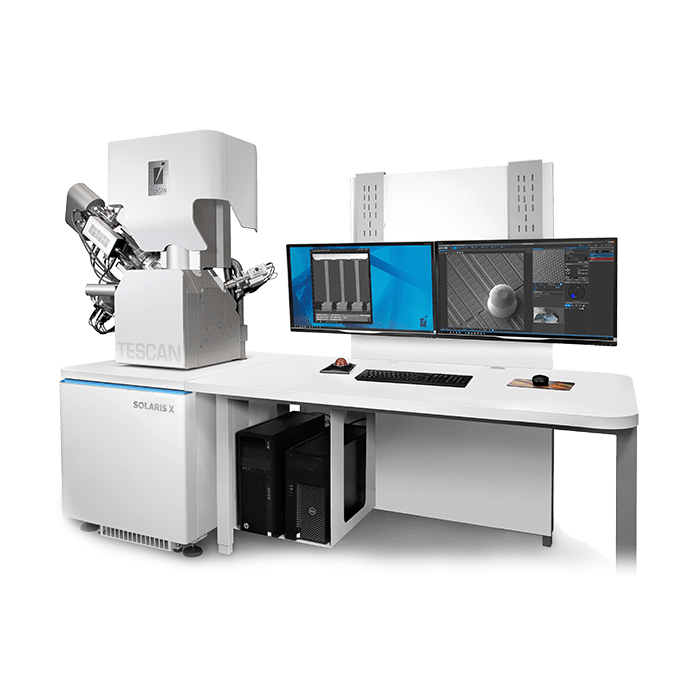
TESCAN SOLARIS X - Xe Plasma FIB-SEM for Semiconductors
EBSDEDSElectron Beam Lithography (EBL)Electron MicroscopyFabricationFIBMicroscopySEMTEMWDS

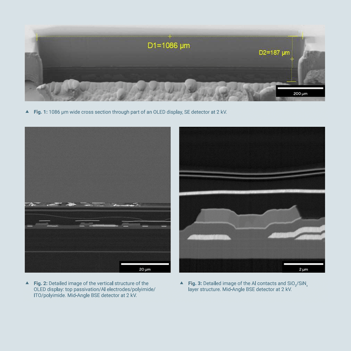
Active Matrix Organic Light Emitting Diodes (AMOLED) displays have become commonplace in smartphone displays. They have a back panel of thin film transistors that makes pixel control more accurate.
Failure analysis of flexible OLEDs materials can be complicated due to the number of materials and layers present. Xe plasma FIB-SEMs like the TESCAN SOLARIS X are ideal for preparing large area cross sections and high resolution imaging. This application note describes how this can be achieved quickly and easily and advantages over more traditional methods like cutting and polishing.
