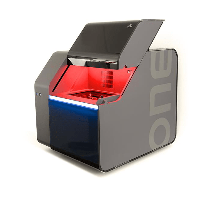
In 1776, Thomas Jefferson declared that “all means are created equal. Unfortunately, the same cannot be said for 3D printers. When it comes to speed and resolution, 2 photon polymerisation (2PP) technology stands head and shoulders above other technologies.
In the area of microfabrication, systems like the NanoOne from UpNano set the standard. The NanoOne is ideal for fabricating parts with complex geometries for academic and industrial research as engineers continue to push the bounds of miniaturisation. As will demonstrated below, it excels at producing precise components, quickly, efficiently and cost effectively, as well as surpassing the limits of micro-stereolithography.
Why is 2PP Technology Ideal for 3D Printing?
The 2PP technology used in the NanoOne allows the highest resolution in the sub-micron range, taking advantage of the spatial selectivity of 2-photon absorption (2PA). Higher spatial resolution is made possible by the fact that 2PA significantly reduces beyond the focus point. This reduces the fluorescence volume, culminating in higher spatial resolution.
The benefit becomes obvious when single and multi-photon beam paths are compared using fluorescent microscopy. As can be seen in the figure, 2PA only occurs at the focal point of the beam, meaning that monomer crosslinking takes place in this plane. Conversely, in the case of single-photon absorption (per stereolithography), emitted light is absorbed along the whole beam.
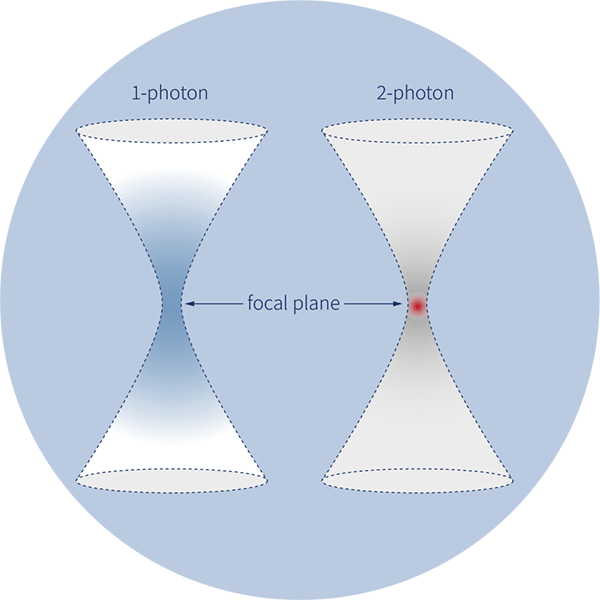
As a result, 2PP enables components to be fabricated in a pre-defined volume with a resolution better than 1µm. Single-photon-based processes can only be created layer-by-layer.
The benefit becomes obvious when single and multi-photon beam paths are compared using fluorescent microscopy. As can be seen in the figure, 2PA only occurs at the focal point of the beam, meaning that monomer crosslinking takes place in this plane. Conversely, in the case of single-photon absorption (per stereolithography), emitted light is absorbed along the whole beam.
As a result, 2PP enables components to be fabricated in a pre-defined volume with a resolution better than 1µm. Single-photon-based processes can only be created layer-by-layer.
Applications of 2PP 3D Printing Technology
The list of applications of 2PP microfabricated components is only really restricted by your imagination. Some examples include:
- Extra cellular matrices
- Lab-on-chip devices
- Optoelectronics
- Photonics
- And more as per the following examples
Filter Elements
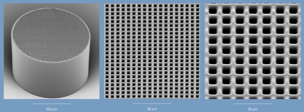
This microporous filter has a diameter of 700µm and height of 500µm. It features 3251 parallel 5×5µm channels. Printing time 13hr 1min, at 300mm/s using fine-mode.
Micro Needles
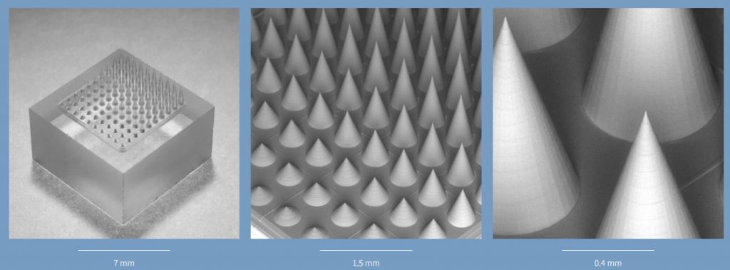
This array of micro needles of varying heights between 260 and 2000µm and 500µm dia. base fabricated using Adaptive Resolution mode. Base area 7.3 x 7.3mm, printing time, base 35min (course mode), needles 4hr 25min (fine mode), print speed 600mm/s.
Micromechanical Components
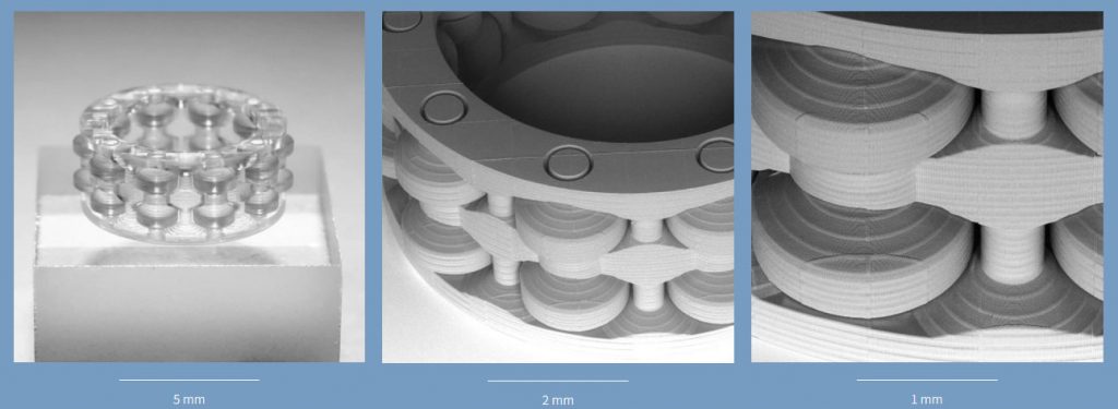
This fully functioning roller bearing was printed in a single print run. It consists of 10 freely moving rollers and a cage. Base area 7.4 x 7.1mm, height 3mm, smallest feature 150µm, print time 1hr 59min at 600mm/s.
Microfluidic Elements
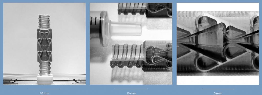
Printed in two halves to reveal the inner flow channels, this 3D Tesla valve prototype includes two full-size female luer-lock connectors. Base area 10 x 5mm, height 40mm, channel width 400µm, printing time 10hr 54 min per half at 750mm/s.
Microlenses
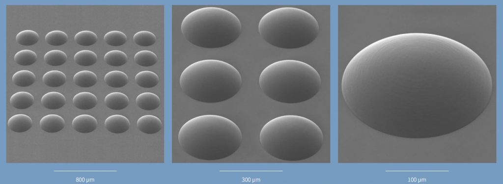
This microlens array consists of spheric microlenses with 300µm dia x 69µm high on a total base area of 1.78 x 1.78mm. This print job took 8hr 51min printed in fine mode with 3 Additional Outlines to produce and excellent surface finish.
Surface Elements
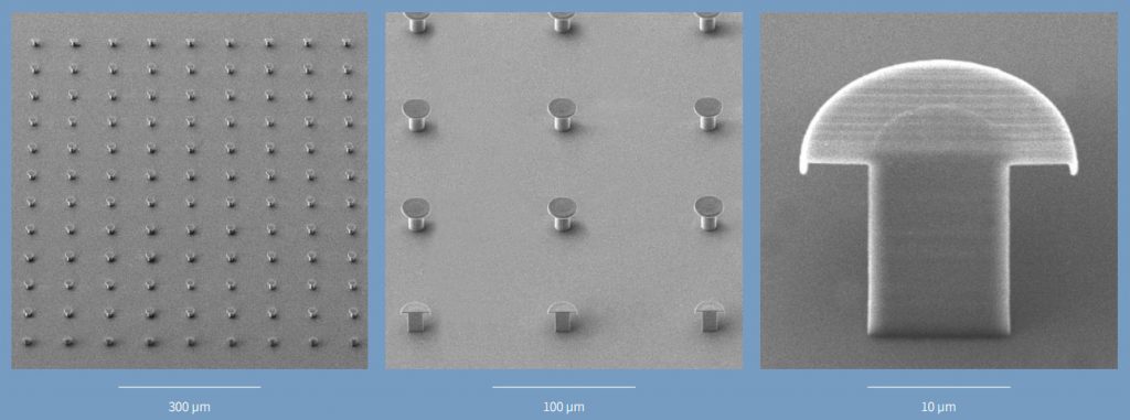
These surface elements were produced to create an ultra-low liquid-solid contact surface, resulting in hydrophobicity. The base area was 1.11 x 1.11mm with each feature being 25µm tall with the smallest feature measuring 760nm. Printing time to produce this surface was 1hr 31min at a rate of 50mm/s. More information is available at in Science at DOI: 10.1126/science.1254787.
What is Possible with 2PP 3D Printing Technology
The 2PP technology used in the NanoOne achieves:
- 170nm resolution – allowing you to fabricate extremely fine structural details
- 1000mm/s and 200mm3/hr – High throughput, even at high-resolution
- Reduced production times
- Low cost/unit – economical fabrication
- Production of relatively large components 40 x 40 x 40mm
The NanoOne can microfabricate features and components across 12 orders of magnitude.

These impressive performance figures are possible with no sacrifice in user-friendliness.
Balancing Speed and Resolution
Adaptive Resolution
The printing process of the NanoOne is optimised for speed using UpNano’s patented Adaptive Resolution. Here, the software classifies the geometry into high and low-resolution regions and adapts the voxel size accordingly, i.e.
- For high volume regions – The laser focal spot is enlarged increasing throughput, at no expense to mechanical properties
- For high-resolution regions – The laser focus reduced to achieve the required resolution
Outline Mode
Another proprietary innovation from UpNano, Outline Mode enables users to create high-resolution, low surface roughness (<10nm) surfaces.
Dip-in Free Printing Modes
Vat Mode – Unique Printing Mode
Unique to the NanoOne, Vat Mode enables the printing of large objects up to 40mm tall.
In this mode a vat with a precision glass window is placed above the objective, isolating the resin from the lens. During the printing process the object is drawn up out of the material vat, while the distance between the print surface and the objective remains constant.

Bottom-Up Mode
In this mode, high-resolution parts can be fabricated directly within the substrate. Here the laser is focussed through the high-precision glass bottom of the substrate and the components is built from the “bottom-up”. Example substrate include petri dishes and microfluidic chips.


