LiteScope - AFM in Your SEM
AFM/SPM/SNOMElectron Microscopy
Correlative in situ AFM and SEM

MoS2 has been of great interest to researchers in recent times due to its unique combination of electronic, optical and mechanical properties. These have attracted the attention of researchers working in areas such as Field Effect Transistors (FETs), photodetectors, solar cells, chemical sensors, supercapacitor electrodes, valleytronic devices and flexible electronics. As such, being able to characterise them at the micro and nanoscale is of great interest to better understanding and controlling their properties.
The LiteScope from Nenovision is an AFM designed to be able to operate within an SEM chamber. As an AFM the LiteScope offers 16 mechanical, electro-mechanical, electrical, magnetic and spectroscopic measurement modes which can be easily correlated with SEM and other related techniques such as EDS. While the complimentary datasets provide a greater understanding of the material under investigation, the two techniques work symbiotically together, with the SEM enabling rapid navigation to regions of interest for further examination by AFM. This streamlines your workflow and prevents the possibility of damaging AFM tips navigating samples.
Furthermore, its ability to be fully integrated into the SEM workflow enables you to simultaneously take AFM measurements while imaging with your SEM, thus accelerating your research by producing richer datasets and providing greater insights into your materials.
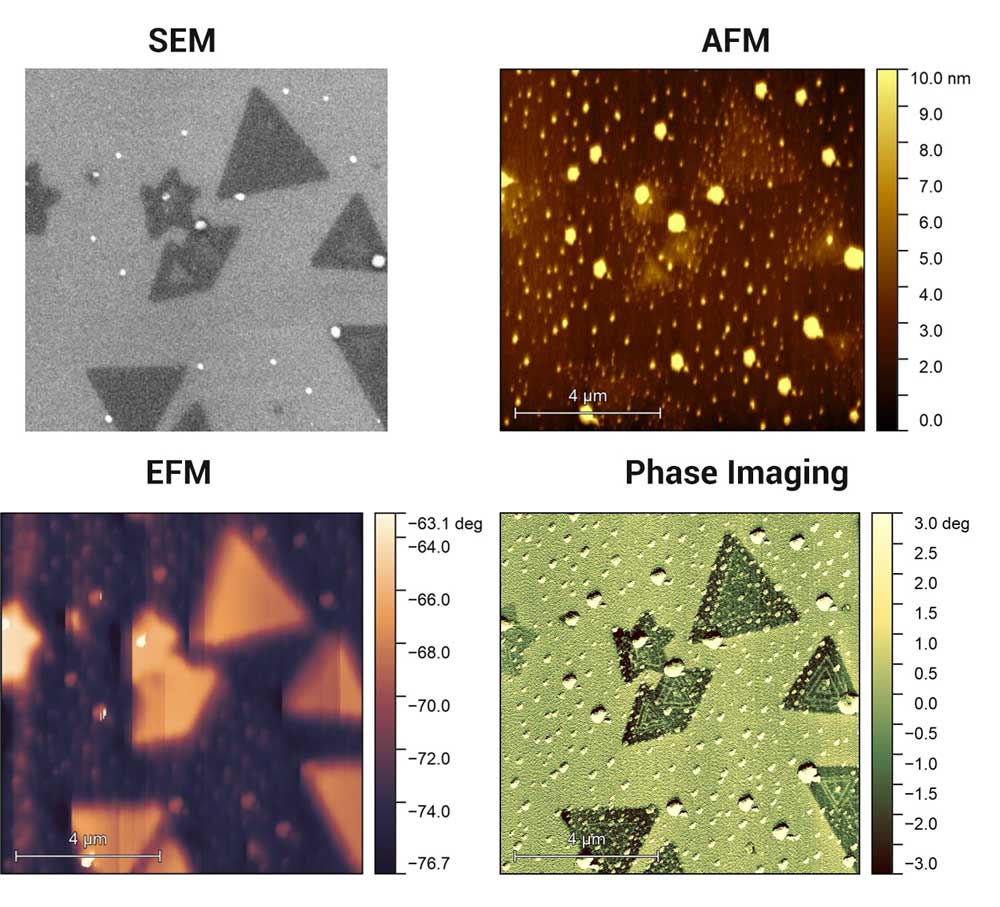
As mentioned, the LiteScope allows you to take multiple scanning probe measurements at the same time. In the example below, researchers were able to simultaneously capture material contrast, surface topography, surface charge distribution, and mechanical properties on sets of samples with different growing conditions of MoS2.
First, they used Scanning Electron Microscopy (SEM) to localise the representative flakes thanks to good material contrast. Using a single probe, they obtained topography information by Atomic Force Microscopy (AFM) about the height of the flakes and discovered a high amount of impurities invisible in SEM. They further obtained qualitative surface charge distribution by Electrostatic Force Microscopy (EFM), and mechanical properties using phase imaging.
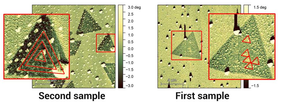
All with one probe (except SEM) on 2 sets of samples, while the software also allows you to easily correlate the complementary datasets. When we compare the results, we see significant differences in phase imaging – see the red triangles, which show centred, resp. random growth of additional layers.
Key values
Features
Using phase imaging – Phase imaging detects edges of MoS2 layers reveals variable growing process of additional layers due to reverse fabrication conditions.