On demand webinar
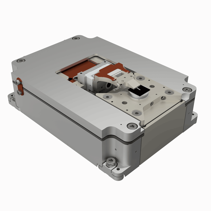
Scanning Electron Microscopy (SEM) and Atomic Force Microscopy (AFM) are two of the most used, complementary techniques for surface analysis at the nanoscale. Combining them by integrating a compact AFM LiteScope™ into an SEM brings novel possibilities for true correlative microscopy and advanced multi-modal sample characterisation that would often be unfeasible using each imaging modality separately.
As there are enormous demands on the higher performance of devices worldwide, material properties have to be measured as complex as possible. For example, structural analysis of multilayered WSe2 flakes on Si nanopillars using Correlative Probe and Electron Microscopy (CPEM) plays an essential role in understanding how the specific shape of the WSe2 monolayer influences the structural performance. As the CPEM technology simultaneously acquires AFM (3D topography, electrical, mechanical, and magnetic measurements) and SEM signals (chemical analysis, FIB/GIS surface modification), the correlated 3D CPEM image provides straightforward data interpretation.

Presenter – Veronika Hegrová
Head of Applications, Nenovision
Veronika Hegrová is the Head of Application department at NenoVision s.r.o. She studied Physical Engineering and Nanotechnology at BUT (Czech Republic) and JKU Linz (Austria), where she continued her work in Nanotechnology. She is interested in high-tech products, their functionalities, and innovations that help to improve sample characterization.
Veronika has co-authored numerouns scientific papers and is especially interested in correlative material characterisation, which accelerates sample characterisation and allows users to focus more on data evaluation. She believes correlative imaging is the next step in helping us better understand complex sample features.


