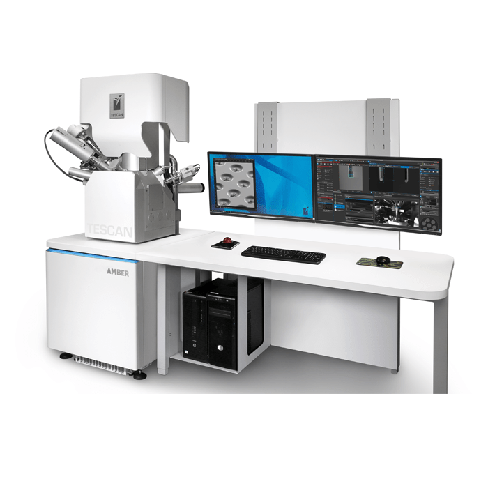
Gallium FIB-SEMs (Focussed ion Beam-Scanning Electron Microscope) have been and continue to be valuable instruments in materials researchers’ arsenals. However, more recent variants like the TESCAN AMBER X, Xe plasma FIB-SEM raise the bar.

Advantages of Plasma FIB-SEMs
The main advantages of plasma FIBs over more traditional gallium FIBs are their ability to remove material at a much faster rate and the fact that they are far less prone to poisoning the material being analysed. Gallium ion implantation can affect chemical analysis via techniques such as EDS (Energy Dispersive X-ray Spectroscopy) or ToF-SIMS (Time of Flight Secondary Ion Mass Spectroscopy) and can alter the electrical and physical properties of the material.
Main Applications of Plasma FIB-SEMs
FIB-SEMs have 3 main applications:
- 3D materials analysis
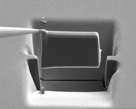
- TEM sample preparation
- Nanofabrication

3D Analysis with Plasma FIB-SEMs
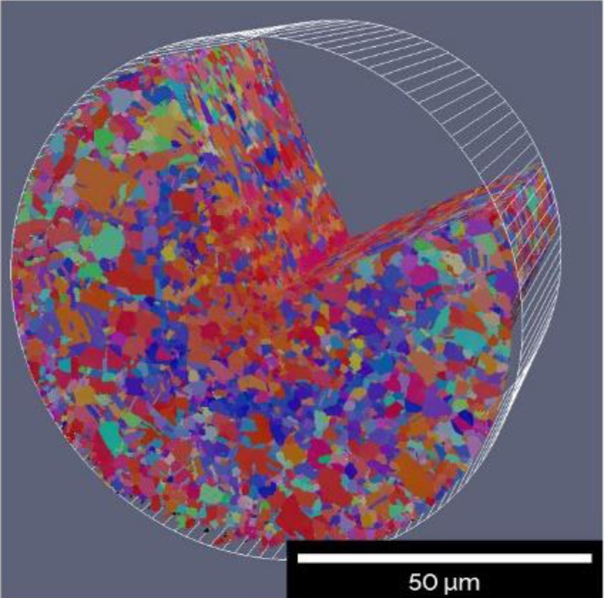
SEMs have the ability to image materials at magnifications far greater than optical microscopes. With the addition of a FIB column, layers can be progressively be removed, while images of each layer can be reconstructed into a 3D model, in a process called FIB-SEM tomography. FIB-SEMs can be equipped with any number of detectors e.g. EDS, EBSD (Electron Beam Backscatter Diffraction) etc., turning them into valuable analytical tools that can perform 3D analyses which can be extremely useful for coatings or materials that vary as a function of depth. Plasma FIB-SEMs can perform these measurements many times faster than gallium FIB-SEMs. While gallium poisoning is avoided, the possibility of xenon poisoning is significantly reduced.

Summary
FIB-SEMs can be used to remove material in a controlled way. This enables users to fabricate nano and micro-scale structures as well as prepare TEM lamellae. Again, the faster material removal rates possible with plasma FIB-SEMs mean higher throughput rates are a reality.
