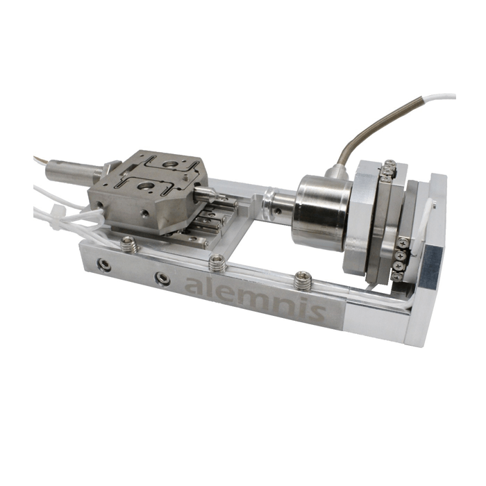
ASA Nanoindenter - Micromechanical Testing System
In situ
White light confocal profilometry

Metrology Module for Hirox Digital Microscope – a complete inspection and measurement solution
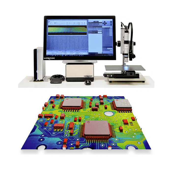
The NPS module is a white light confocal point sensor. When coupled with a high-precision motorised stage it enables non-contact sub-micron altitude/Z-measurements on any surface resulting in a 3D surface.
It affords a wide range of measurement modes on 2D profiles and 3D shapes including various roughness parameters, sphericity, curvature, length, height, radius, angle, volume and much more. Analyse regions up to 4000µm and correlate these back to manufacturing/design specification.
ISO 25178-602 is an accepted technique for the determination of surface roughness using white light chromatic confocal technology and is used in labs all over the world. NPS satisfies these requirements and enables measurement beyond the limitation of optical depth of field.
A wide array of NPS sensors are available depending on your specific application. These provide seamlessly integrated, high accuracy measurements. The general rule of thumb is:
The following table represents some of the options that are available to you.
| NPS1 | NPS2 | NPS3 | NPS4 | NPX | |
|---|---|---|---|---|---|
 |  |  |  |  |
|
| Measuring range | 150µm | 400µm | 1400µm | 4000µm | 1000µm |
| Working distance | 3.3mm | 10.8mm | 12mm | 16.2mm | 18.5mm |
| Max. sample slope | 42.5° | 28° | 25° | 21° | 44° |
| Lateral resolution | 1µm | 1.8µm | 2.6µm | 4.6µm | 2.5µm |
| Height accuracy | 20nm | 45nm | 150nm | 300nm | 100nm |
| Roughness suitable | Yes | Yes | Yes | Yes |
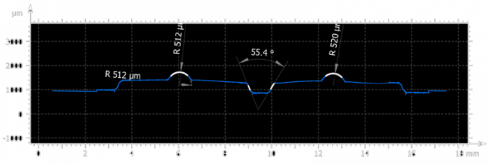
The fastest measurement mode. Simply scan between 2 points and from the profile and measure horizontal & vertical distances as well as Ra, Rz and Rt measurements. You can also measure several profiles and combine the data into a single report.
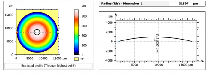
After scanning a surface region you can easily determine shape and geometry data. E.g. the curvature of spherical objects. On other shapes you can easily measure length, height, radius, angle, volume and much more across areas up to 4000µm.
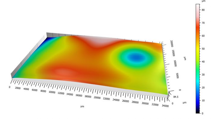
Easily assess warp, deformation, waviness or flatness over regions up to 500x500mm using with the NPS and the XY stage.
You can also measure defects that can occur from machine or processes such as work anomaly, residual stress, vibrations or heat treatment.
Coplanarity can also be determined on profiles or surfaces.
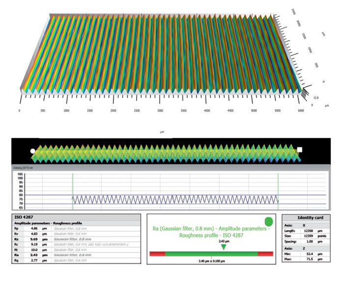
Surface metrology is used to determine surface topography which in turn dictates if a part meets design specifications and tolerances. This can dictate whether a part is fit for service. Measurements include profile roughness (Ra), surface roughness (Sa), surface texture, asperity and structural characterisation.
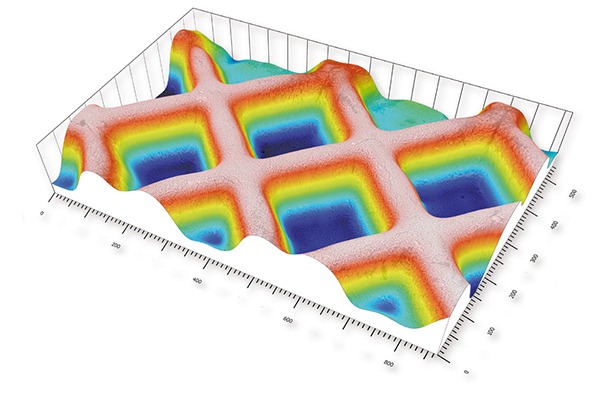
Benefit from the most advanced metrology solution available, MountainsMap® from Digital Surf which provides:
