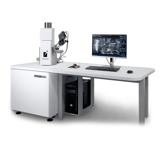
ProbeWorkstation for Electrical Characterisation of Semiconductors

The latest tool for high-precision in-situ electrical nanoprobing.

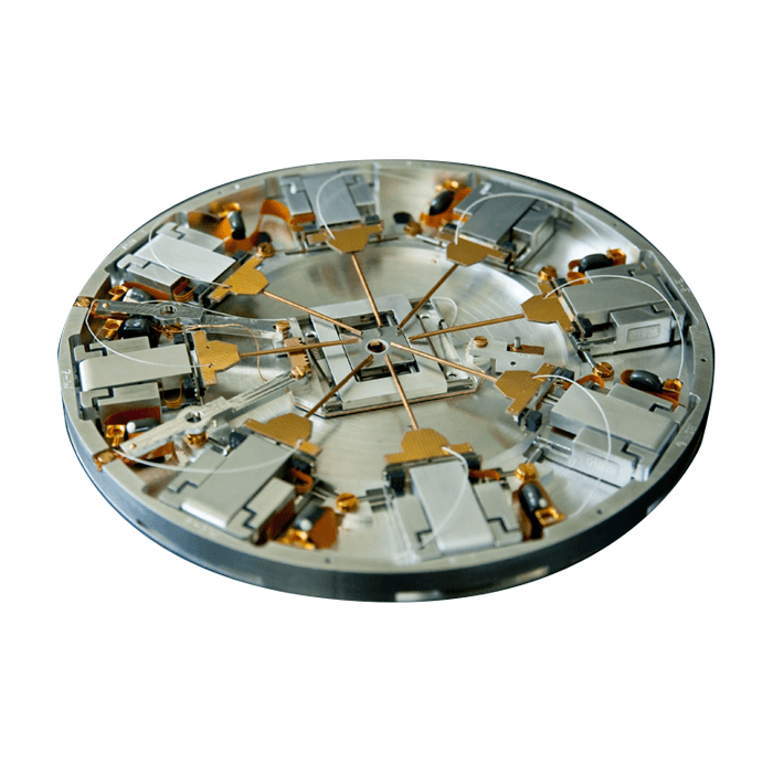
The ProbeWorkstation is a powerful, dedicated system for electrical characterisation of semiconductor devices and advanced materials in SEM and FIB. The optimal combination of our market-leading nano-manipulation and probing products provide a versatile, integrated solution for failure analysis and R&D applications requiring stable, low-current measurements.
  • Key Features

    • Unmatched stability and precision. Compact, extremely stable design guarantees < 1 nm/min drift with no backlash, creep or reversal play.
    • Load-lock compatibility. SEM and FIB load-lock compatibility allows for fast cycle times and increased chamber cleanliness and simple integration into your existing SEM or FIB/SEM tool.
    • Single unified software interface (APT) for driving the probe tips and controlling all measurement functions (incl. Keithley 4200 operation) and allowing for electrical fault isolation using EBIC, EBAC, EBIV, RCI, EBIRCH, etc. Easy integration using the microscope‘s auxiliary video input, EBIC image acquisition by SEM software.
    • In-situ circuit editing. Capable of probing at FIB tilt angles for in-situ circuit edit applications and with a low profile design allows for small working distances down to 2 mm - enabling low-kv imaging.
  • Loading the PS8 ProbeWorkstation into an SEM

    Run time – 47 sec

    The quick demonstration chows how simple it is to load and retrieve the Kleindiek PS8 Probe Workstation into an SEM.
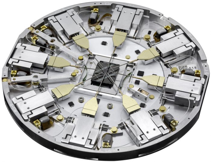
  • Kleindiek PS8e fully encoded ProbeWorkStation

    PS8e – Fully Encoded Prober Shuttle with 8 Probes

    The latest iteration of the Prober Shuttle platform now features positional encoders for all 27 axes of motion.

    The introduction of encoders yields a significant reduction in the time to result as the probe tips can be prealigned at the push of a button. A list of user-definable store points allows operators to (re-)address specific locations on the sample. Moving all eight probes and the substage from parked positions back to their
    respective working positions is completed in approx. one minute.

    Download the PS8e Brochure

  • All
  • AFM/SPM/SNOM
  • CL
  • CLEM
  • Diffraction Imaging
  • EBSD
  • EDS
  • Electron Beam Lithography (EBL)
  • Electron Microscopy
  • Fabrication
  • FIB
  • Hyperspectral
  • In situ
  • Micro XRF
  • Microscopy
  • Raman
  • SEM
  • Spectroscopy
  • TEM
  • Thermal Probe Lithography
  • WDS