AttoMap

Compositional Analysis and Microscopy with X-ray Fluorescence Technology Complementary to Synchrotron Performance

Redefining µ-XRF with the world’s first X-ray Fluorescence Microscope, enabled by Sigray Patented Technology
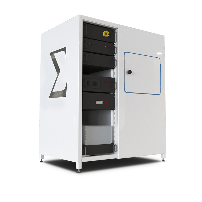
  • Sigary Attomap 200 microXRF

    Key Features

    • Highest resolution x-ray fluorescence mcroscope spatial resolution down to 5 μm
    • Highest throughput x-ray fluorescence microscope down to 5 ms/point
    • Unprecedented PPB sensitivity within 1 second, up to orders of magnitude higher in sensitivity than alternative techniques such as SEM-EDS
    • High brightness x-ray source 50X brightness of microfocus sources used in conventional μXRFs
    • Easy to use and powerfully precise simultaneous detection of multiple elements and no sample preparation required
    • Fine Anode Array Source Technology (FAAST) Sigray's unique multi-target source provides easy software-selection of target materials to ensure the ultimate sensitivity for each element
    • Patented Trace Mineralogy Technique Femtogram and < 1ppm sensitivity for trace elements. Orders of magnitutde higher sensitivity than SEM-EDS
    • GeoFocused edition provides chemical mapping mining, geochronology, exploration with simultaneous acqutistion
    • Patented Multi Energy Approach maximise element sensitivity using a push button change of source and optic

Applications

  • Mineralogy
  • Life sciences & metallomics
  • Contaminants & impurities in industrial processes e.g. batteries
  • Semiconductor
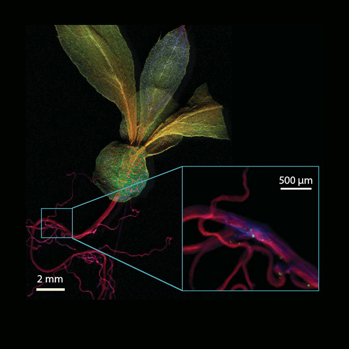
  • Environmental/botany

AttoMap Models

AttoMap-200
AttoMap-310
Sigary Attomap 200 microXRF
Sigray Attomap 310 microXRF
Spatial resolution
Down to 3-5 μm with high resolution optic. 7-10 μm with standard optics.
Sensitivity
Sub-ppm relative detection sensitivity. Picogram to femtogram absolute sensitivity.
Variable Angle Acquisition
3 degrees (near-grazing) to 90 degrees (normal) in 0.01 degree increments.
X-ray source
Sigray patented ultrahigh brightness sealed microfocus source
X-ray targets
Up to 5 targets.
Includes selection from Si, Cr, Cu, Rh, W, Mo, Au, Ti, Ag.
Others available upon request.
Power | Voltage
50W | 20-45 kVp
X-ray optic
Sigray proprietary double paraboloidal x-ray mirror lens
Transmission Efficiency
~80%
Magnification
1:1 magnification default
Demagnifying optics for higher resolution available upon request
Interior Coating
Platinum for increasing collection efficiency of optic
X-ray detector
SDD Detector
Energy Resolution
<129 eV at Mn-Ka
Stage Travel
100 x 100 mm (upgrades available upon request)
200 x 200 mm standard
300 x 300 mm for semiconductor wafers
Other Modalities
Integrated optical microscope and transmission x-ray microscope for alignment
Brochure
AXT Download brochure