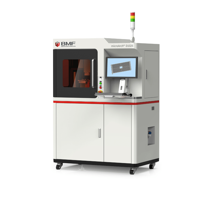
microArch Hybrid Resolution 3D Printers
Additive Manufacturing
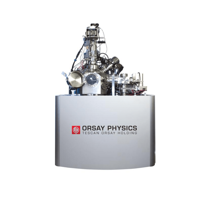
A versatile platform ideally suited to FIB-SEM applications in an UHV and contamination free environment

A specially designed platform combining UHV required applications such as MBE, ToF SIMS etc … with the resolution power of a SEM & FIB

Nanospace is the solution you have been looking for, if you need a contamination free and versatile platform that integrates various ion species and a high-resolution SEM. NanoSpace is a fully customisable UHV chamber that serves as the platform for you to build your own bespoke experimental setup. Its modular architecture allows you to integrate a wide range of options, some of which are outlined below.
Some potential applications for the UHV FIB-SEM Nanospace might include:
Nanospace UHV FIB-SEM chambers are compatible with a range of ion columns depending on your application. These include:
| FIB Column | Ion Species | Max. probe current | Notes |
|---|---|---|---|
| i-FIB plasma | Xe+ / Ar+ / N2+ / He+ / O2+ | 3 µA | Plasma FIB column, Ga free, high-resolution and powerful |
| Orage | Ga, Au, Ge, Si, Gold clusters Bi+, ... | 100 nA | LMIS FIB column, Ultra-high resolution optimised for high current and low kV imaging/milling |
| Cobra | Ga, Au, Ge, Si, Gold clusters Bi+, … | 50 nA | LMIS FIB column, high-resolution and versatile |
| Chroma | Ga, Au, Ge, Si, Gold clusters Bi+, … | 50 nA | LMIS FIB column, “pentode” objective design, highly customisable |
| Taipan | Ga | 20 nA | LMIS FIB column for correlative Optical / FIB column |
You can choose between:
depending on your imaging needs and materials requirements.
Nanospace columns are configured with multiple ports optimised for a range of detectors such as:
If you are looking for a system for performing in situ measurements and dynamic studies, Nanospace caters for this as well. Some examples might be:
