Abstract
Extreme ultraviolet (EUV) light offers the ability to characterise many different properties of materials, including those relating to their nanoscale structure and quantum state. But to date, EUV light as an illumination source for microscopy and numerous other physical characterisation methods has mainly been restricted to the domain of the synchrotron. The possibility of a versatile multi-modal lab-based system using an EUV source is now becoming a reality in the form of the KMLabs QM Quantum Microscope™. The first such system is currently being developed in collaboration with IMEC, the world leading research institute based in Belgium, and offers exciting possibilities for imaging and analysis of materials at the nano and quantum scales.
Introduction
There are a vast number of microscopy techniques available today that use various wavelengths of electromagnetic radiation ranging from IR through to X-rays and electrons. Use of a specific wavelength range of illumination is typically dictated by the application and the properties under investigation.
The wavelength range of 6~120 eV, incorporating the Vacuum Ultraviolet (VUV approx. 6~30eV) and the Extreme Ultraviolet (EUV, approx. 30~120eV), is well noted for its typically strong interactions with materials. Characteristic absorption, scattering, or reflection behaviour, for example, has great potential to provide a wealth of information on materials including insight into their chemical, physical, mechanical, magnetic, and thermal properties. Furthermore, the strength of these interactions combined with the short wavelength of light brings unique opportunity for functional imaging applications.
Until recently, these capabilities have had limited exposure outside of synchrotrons as a lab-based EUV source has not been commercially available. However, KMLabs has developed a tuneable, coherent EUV source based on high harmonic generation that has the potential to open the door for lab-based microscopy using VUV/EUV radiation in a routine manner.
Advantages of EUV Radiation
The utilisation of EUV light in a laboratory setting to perform various optical experiments has been largely underexplored due to challenges associated with generating and manipulating photons in this portion of the electromagnetic spectrum. Nonetheless, as a light source for microscopy coherent EUV photons from a pulsed laser source offer some unique capabilities:
- Strong elemental and chemical contrast particularly for low-Z compositions, due to substantial material-photon interactions at low energy
- Penetration of near-surface multilayers and films with high sensitivity to thickness, composition, and interfaces
- High spatial resolving power resulting from short wavelength light
- Flexible sample requirements, with little or no sample preparation required and an uncharged imaging probe (photons, as compared to electrons or ions for example)
- Potential to capture femto- to picosecond dynamics with ultrafast laser pulses in the EUV range
The QM Quantum Microscope
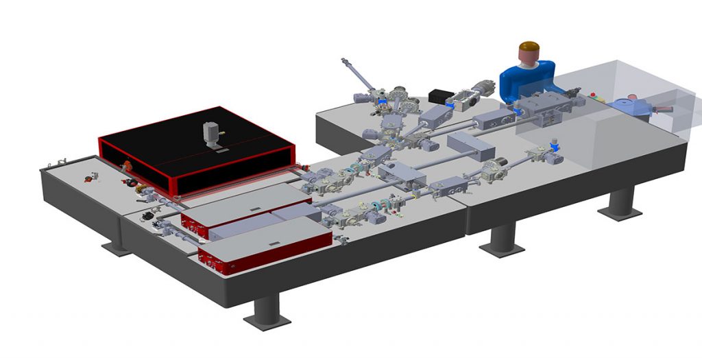
The QM Quantum Microscope is a new platform developed to harness the power in this range of the electromagnetic spectrum, by integrating light sources and experimental stations to elucidate critical details of crucial technology problems. The first of its kind system, developed in collaboration with IMEC, aims to realise this untapped potential by combining the time sensitivity of femtosecond short-wavelength lasers with the spatial resolution of EUV microscopy and diffraction, thereby enabling a series of techniques tuned for critical problems in both research and industry. For example, for batteries EUV absorption near the lithium edge can provide a microscopic and spectroscopically rich area to understand lithium bonding and electrode evolution. For semiconductors, microscopy at the nano to quantum scale has the potential to provide critical details on buried and surface nanotopography and multilayers in new ways that aren’t accessible with existing techniques. As such, with the potential to provide next generation imaging and analytical capabilities that delve into the quantum realms, the term QM Quantum Microscope has been coined to describe a cutting-edge collaborative effort

to provide a
microscopy and characterisation platform built around decades-long developments
and deep expertise in the tuneable laser source.
Beyond the source, the other key component required
to realise the potential of the QM Quantum Microscope is the coherent diffraction
imaging (CDI) chamber, where diffraction patterns reflected from the sample
surface can be acquired and reconstructed to yield full field of view, high
resolution images. To further maximise
the value of the light source, additional experimental stations can be integrated
as well in a multi-beamline configuration, enabling the system to serve as a
flexible and powerful platform for diverse needs of multiple users and
applications all benefiting from the unique possibilities in the EUV range. Possible experimental methodologies include:
- Coherent diffraction imaging (CDI)
- Pump probe spectroscopy, including IR pump/EUV probe diffraction imaging for thermomechanical and elastic behaviour of nanoscale structures
- Magnetic dynamics, MOKE (Magneto-Optic Kerr Effect) diffraction and magnetic imaging with elemental sensitivity to spin in Fe, Ni, Co
- ARPES – Angle-Resolved Photoemission Spectroscopy
- Reflectometry
- COLTRIMS – Cold Target Recoil Ion Momentum Spectrometry
Scientific Opportunities with the QM Quantum Microscope
The multiple imaging and characterisation modalities enabled by the QM Quantum Microscope hold great potential for materials characterisation with new insights into structure and behaviour at the nano to quantum scale:
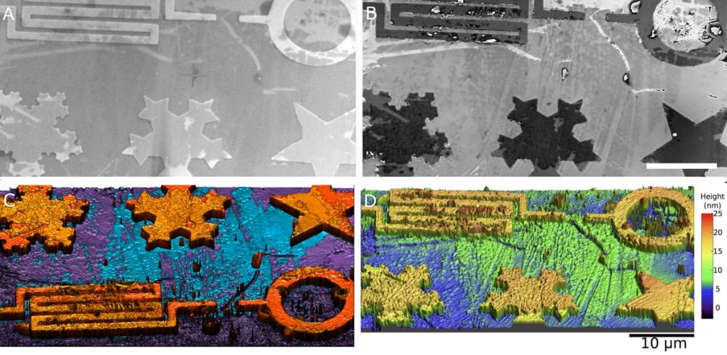
- 2D high contrast imaging of composition and structure: Surface and near-surface imaging providing full field amplitude and phase contrast maps over tens of microns field of view. The EUV range offers the potential for high sensitivity to oxide layers, dopant profiles, and magnetic/elemental/chemical contrast. Small phase shift variations in reflected light also provide topographical mapping for height variations in the sub-nanometer regime.
- Mechanical properties of patterned films: Acoustic behaviour at the nanoscale interrogated by pump-probe methods contains information describing elastic properties, strain, and mechanics for structures down to few nm length-scale; difficult or impossible to access with physical mechanical characterisation methods.
- Materials properties and dynamics: Transport, magnetic, electronic and elastic properties of materials and nanostructured media can be observed via their femto- to picosecond time response using ultrafast laser pulses
- Functional characterisation of spintronic, ALD, 2D, low-density lightweight, energy, space and photovoltaic materials
Imaging Demonstration and Applications

In the microscopy toolkit, multiscale and multimodal approaches are being increasingly employed to understand sample characteristics across a range of length scales and descriptors. As a newly developed technique, CDI in the EUV range complements and builds upon existing methods by adding new information that was previously difficult or impossible to access.
EUV light generated from laser sources is spatially coherent and offers a degree of energy tunability, much like synchrotron radiation. And, like many synchrotron experiments, in some instances the incident beam can be tuned around absorption edges in materials, offering the ability to see a range from surface to sub-surface effects, as well as enhance sensitivity to the interactions with particular elements or compounds. Building upon an example mentioned previously, a simple yet powerful instance of using this spectral effect is related to bonding states in lithium, which can be imaged via the strong compositional dependence in the EUV around the Li K-edge (at about 55 eV). With this approach, compositional variations in battery electrodes or interfacial layers can be identified and quantified.
Another promising use case is in surface metrology for semiconductor devices: the reconstructed intensity and phase signals describe sub-nm height variations as well as surface composition at ~10s of nm spatial resolution. This could provide another independent data source for computational metrologies, and a unique view of the surface features, particularly patterned structures. As compared to AFM, the penetration depth would allow direct imaging through layers in some cases, or into deep recesses of high aspect ratio areas where an AFM tip is limited. Furthermore, the lack of charged particle interactions, as compared to a technique like scanning electron microscopy, is attractive for capturing edge features or corners where charging artefacts may otherwise prove problematic. The sum of these traits yield a profoundly novel tool in measuring surface and subsurface roughness inside critical features relevant to device performance.
Summary
The challenges with producing, manipulating, and measuring EUV light in the laboratory have traditionally limited many experiments in this portion of the electromagnetic spectrum to select synchrotron facilities. Recently, with the introduction of the QM Quantum Microscope powered by KMLabs’ tabletop EUV laser solutions, new opportunities are emerging for optical experiments where the scientific focus is shifting away from the operation of the instrument and towards the interpretation of the results and new insights they produce. Coherent diffraction imaging offers unique contrast information and low-Z sensitivity for surface and near-surface features, and pump-probe ultrafast spectroscopy elucidates the dynamic behavior dictating the functionality in a range of nano and quantum scale materials. With ongoing collaboration and maturation of the experimental equipment, KMLab is aiming to foster development of the QM Quantum Microscope that would herald the next major step in materials microscopy and analysis.
