
The TESCAN AMBER X 2 delivers advances in plasma FIB technology combining the benefits of Ga FIBs and plasma FIBs
TESCAN, in collaboration with Orsay Physics, announces the launch of TESCAN AMBER X 2, a groundbreaking plasma FIB-SEM system designed to set new standards for materials science research. This state-of-the-art technology offers unmatched resolution, throughput, and versatility for comprehensive sample preparation and characterisation.
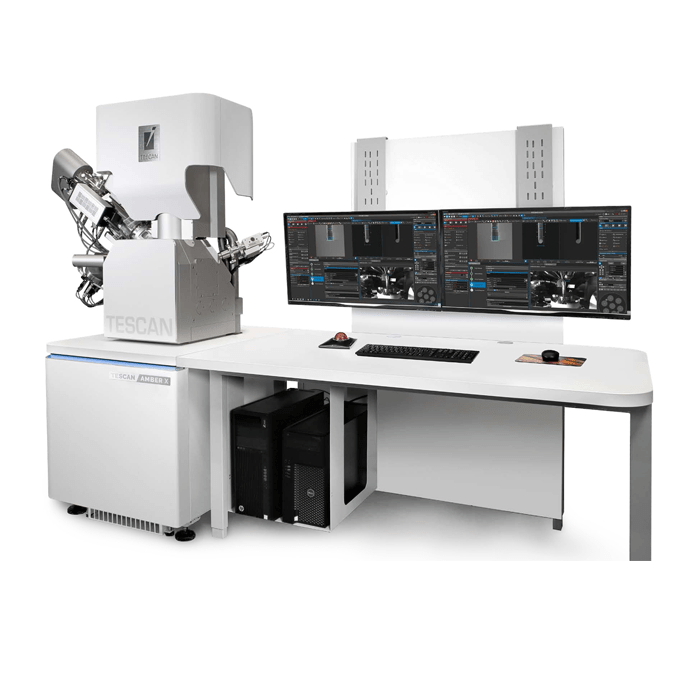
The TESCAN AMBER X2 represents a revolutionary advancement in Focused Ion Beam Scanning Electron Microscopes (FIB-SEMs), seamlessly blending the precision of Ga FIB-SEMs with the efficiency of plasma FIB-SEMs. This innovative solution delivers unparalleled resolution, making plasma FIB utilisation as effective as Ga FIB-SEM. It also enables rapid large-scale milling, facilitating the acquisition of high-quality, multimodal 2D and 3D statistical data acquisition from areas as large as hundreds of micrometers.
TESCAN AMBER X 2 leverages Orsay Physics’ extensive expertise in plasma FIB-SEM technology, offering significant benefits for materials science applications, namely increased precision enabling fully automated TEM/STEM specimen preparation, and enhanced milling efficiency.
The new FIB column is married to TESCAN’s BrightBeam™ field-free SEM column which offers ultra-high-resolution imaging capabilities for metallic, magnetic, non-conductive, charging, and beam-sensitive specimens, providing accurate analysis – even at low keV. Furthermore, it enables multimodal and multiscale materials characterisation capabilities, providing an all-encompassing solution for researchers and a perfect system for multi-user facilities and central laboratories.
Key Features:
- MISTRAL Plasma FIB Column™: Optimises beam parameters for superior beam profiles, simplifying workflows and improving precision, beam placement accuracy at low ion beam energies and milling performance
- TEM AutoPrep Pro™: Fully automated workflow for precise and efficient TEM sample preparation
- Field-Free UHR-SEM Column: Allows high-resolution imaging of diverse materials, eliminating the limitations of immersion optics, while offering a wide field of view and various scanning modes
- Multimodal and Multiscale Analysis: Supports unique 3D methods like 3D ToF-SIMS for detailed elemental composition analysis, crucial in applications such as next-generation battery research, as well as 3DEDS and 3DEBSD
Martin Slama, Product Marketing Manager for the TESCAN AMBER X 2, commented, “We are thrilled to introduce the TESCAN AMBER X 2 plasma FIB-SEM to the materials science community. This innovative product delivers high-resolution, high-throughput characterisation and automation for TEM/STEM sample preparation, disrupting the traditional position of Gallium FIB-SEMs in multipurpose materials characterisation laboratories.”
Following its initial announcement at the M&M 2024 conference in Cleveland, Ohio, the TESCAN AMBER X 2 will be unveiled officially on August 25th at the EMC conference in Copenhagen. TESCAN will be offering demonstrations at EMC where you will be able to experience its full range of capabilities. Closer to home, one of the first TESCAN AMBER X 2 systems will be delivered to the University of Sydney in the coming months.